


Thick Film Printed Ceramic Substrates Manufacturer in Pune
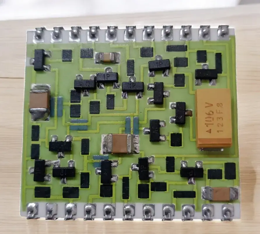
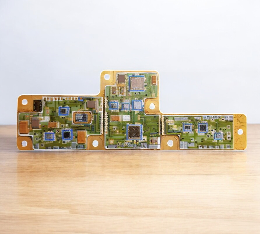
Thick film substrates manufacturing uses screen printing and firing technology. The base material required for thick film substrates is 96% alumina on which conductive, resistive and insulating pastes containing glass frit, deposited in patterns by screen printing and fired at high temperature. The thicknesses of fired films are typically in the range 8–20μm thick hence called thick film substrates. The Resistivity range is 10Ω/square to 1MΩ/square and films can be built in multilayer structure.
Laser Scribing, Profiling & Via Drilling Process
Scribing is a process where a line of laser pulses is fired into the material and 30–50% of the material is removed; this weakens the substrate, and substrate can easily be divided into single units. Profiling is, for example, used a lot in sensor fabrication, where a circuit needs to fit round tubes or other different complex shapes. Drilling of holes can provide a "via" (conductive link) between the two sides of the substrate, normally hole sizes are in the range 0.15–0.2mm.
Applications
Thick Film Printed Ceramic Substrates are widely used in RF/microwave circuits, hybrid microcircuits, power modules, and aerospace & defense electronics where high thermal stability and precision resistor/conductor patterns are essential.