
There are multiple methods for the deposition of material on a ceramic substrate. DC (Direct Current) or RF sputtering is a thin film Physical Vapour Deposition (PVD) coating technique in which a target material used as the coating is bombarded with ionized gas molecules, causing atoms to be sputtered into the plasma. These vaporized atoms then condense and deposit as a thin film on the substrate to be coated. Depending on the requirement, two or three layers can be sputtered using a sputtering machine. A metallized substrate size of 4" × 4" is a good choice for optimum cost during the development and production of thin film substrates.

Thin Film Sputtered And Patterned Ceramic Substrates
Thin Film Sputtered And Patterned Ceramic Substrates
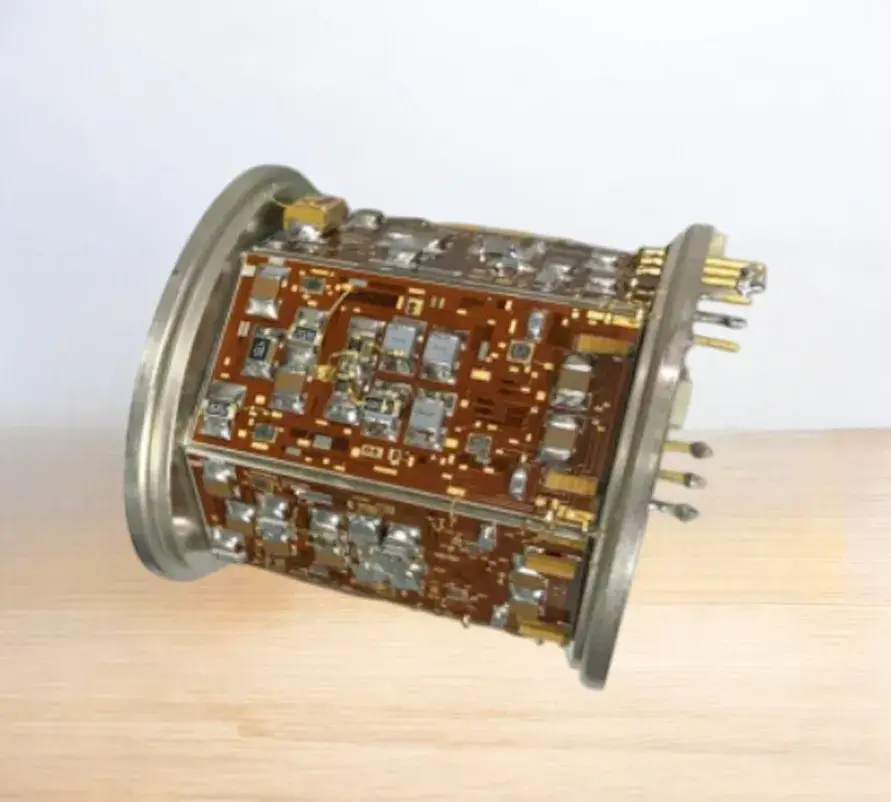
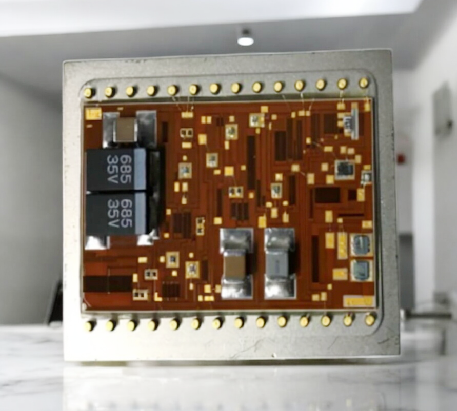
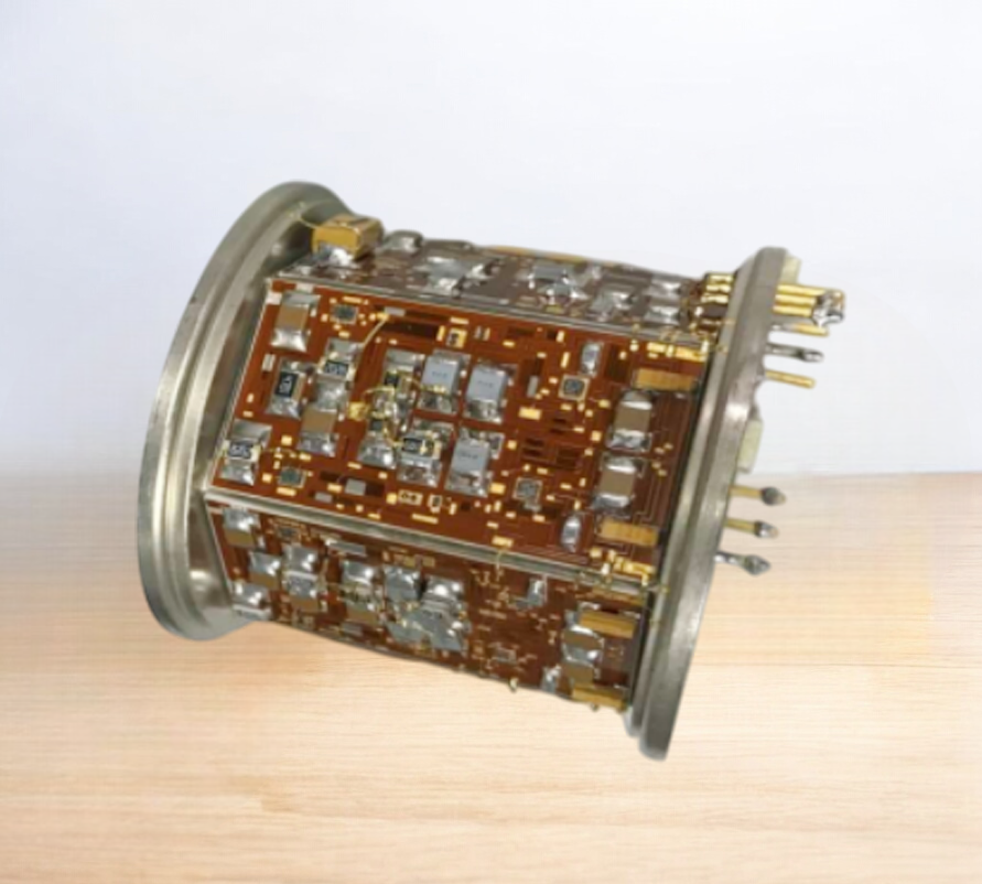
Thin film substrates used in microelectronics products are fabricated on ceramic or insulated substrates by depositing materials in thin layers of less than 1 micron. These layers can be conductive or resistive depending on the application. These metallized substrates are then patterned to form microcircuits using masking, etching, and plating processes. The advantage of thin film technology is that better resolution and higher circuit density can be achieved. These substrates are widely used in specialized and RF applications.
Thin film capabilities
-
Substrate Materials: Alumina, Quartz etc
-
Adhesion Layers: Adhesion – Titanium , Chromium etc
-
Resistive layers – Nicr, NicrSi
-
Conductor layers : Copper
-
Resistor Parameters: Resistivity: 25 ohm/Sq to 1 Kohm /Sq
-
TCR: -100 to +50 ppm/oC
-
Tolerance : 0.2% to 20%
-
Minimum Dimensions : 50 µ